Course Overview
An intensive, transistor-level design project focused on creating a complete EEG signal processing module supporting end-to-end EEG acquisition and conversion. The architecture encompasses a preamplifier, a sampling module, a single-slope analog-to-digital converter (ADC), and a digital-to-analog converter (DAC).
Core Project: End-to-End EEG Signal Processing Module
Designed and simulated a comprehensive integrated circuit module from the ground up, focusing on the precise amplification and digital conversion of weak biological electrical signals.
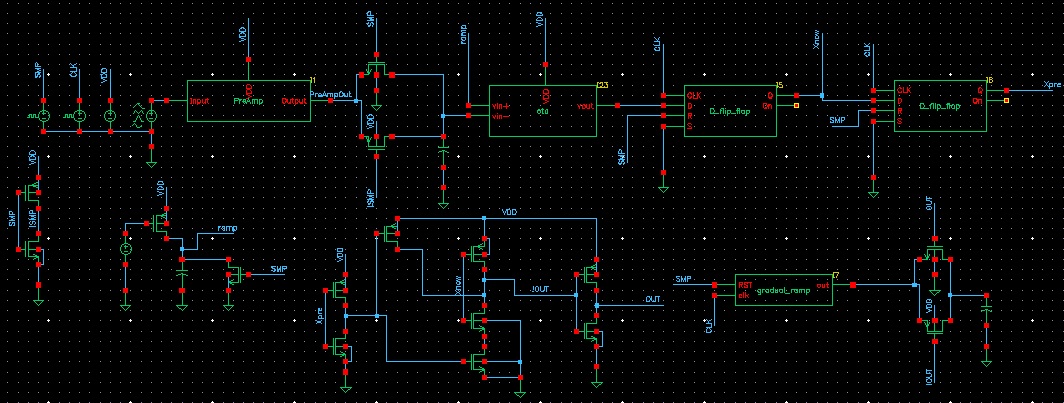
1. Preamplifier Design
Architected a folded cascode operational transconductance amplifier (OTA) for initial signal amplification and level shifting.
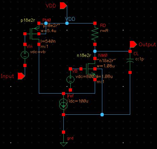
- Dynamic Range Optimization: Configured key control parameters (R = 20k, vb = -15mV) to successfully map the weak input signals to an output range of 0.7V to 1.6V.
- Saturation Prevention: Ensured the mapped output perfectly matched the valid input range of the subsequent ADC comparator, actively avoiding signal saturation. Maintained a strict linear input/output relationship to guarantee signal fidelity.
Output/Input YvsY Curve and Input Distribution Histogram of the Preamplifier: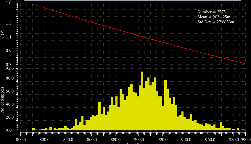
2. Sampling Module
Engineered a discrete-time sampling circuit utilizing a PMOS, an NMOS, and a holding capacitor.
- Charge Transfer & Timing: Utilized the SMP signal to control the MOSFET switches, charging the capacitor during high levels and maintaining the voltage during low levels.
- Parasitic Mitigation: Identified and neutralized an abnormal voltage increase during the holding phase by deliberately integrating a significantly larger capacitor into the design to stabilize the sampling voltage.
3. Single-Slope Analog-to-Digital Converter
Integrated an optimized ramp generator, a five-transistor OTA comparator, and custom digital logic to convert analog voltages into precise digital time sequences.
- High-Linearity Ramp Generator: Analyzed the convex distortion caused by channel length modulation. Mitigated this effect by substantially increasing the PMOS channel length and utilizing a large capacitor to stabilize the input current, producing a highly linear reference ramp (vrampb = 1.5046V).
The Output Waveform of the Ramp Generator (Purple) and the Counter (Blue):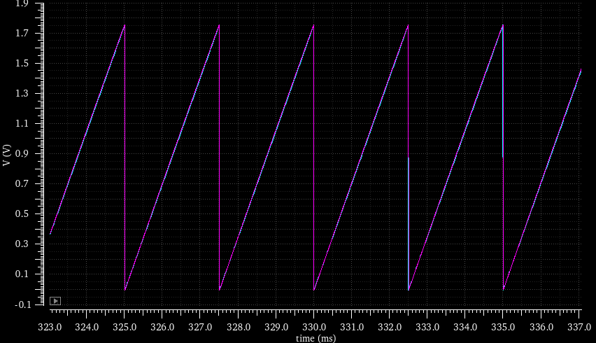
- Rising Edge Detection: Designed a precise edge detection circuit using two D-flip-flops, two NOT gates, and one AND gate to capture the exact moment of comparator state inversion and latch the digital sequence.
- Five-transistor OTA Comparator: The comparator is engineered to continuously evaluate the differential between a sampled analog EEG voltage and a highly linear reference ramp voltage. Because the preceding preamplifier stage strictly maps the input signal to a 0.7V to 1.6V range, this OTA was specifically optimized to maintain high gain and stability within this common-mode input range. Operationally, as the ramp generator’s voltage linearly increases and intersects with the held sampled voltage, the differential input polarity shifts. This causes the OTA’s output state to swing sharply, generating a precise trigger signal.
The Comparator Design:
4. Digital-to-Analog Conversion & System Optimization
Reconstructed the analog signal using a counter and switching transistors, and performed deep system-level tuning to minimize latency.
- Signal Reconstruction: Verified through transient analysis that the final DAC output accurately maintained the input signal without offset errors.\
- Latency Suppression Architecture: Addressed the inherent delay of the single-slope ADC by applying a 0.7V reference voltage to the ramp generator (aligning digital 0 with the preamplifier’s minimum output) and aggressively increasing the CLK signal frequency to 500kHz. Adjusted vrampb to 1.4623V to maintain waveform consistency, drastically suppressing overall system delay.
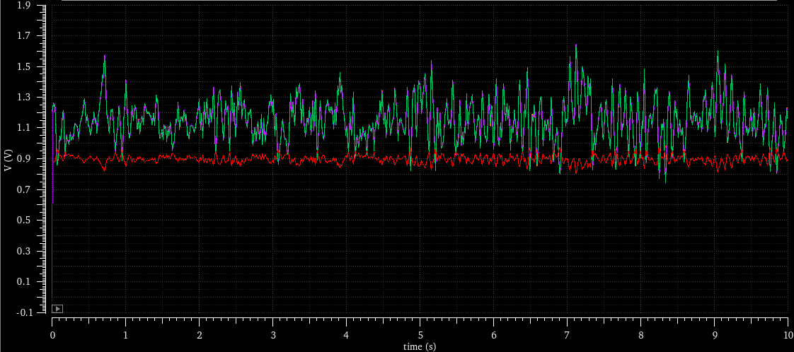
Final Output (Purple), Input (Red) and Preamplifier Output (Green):
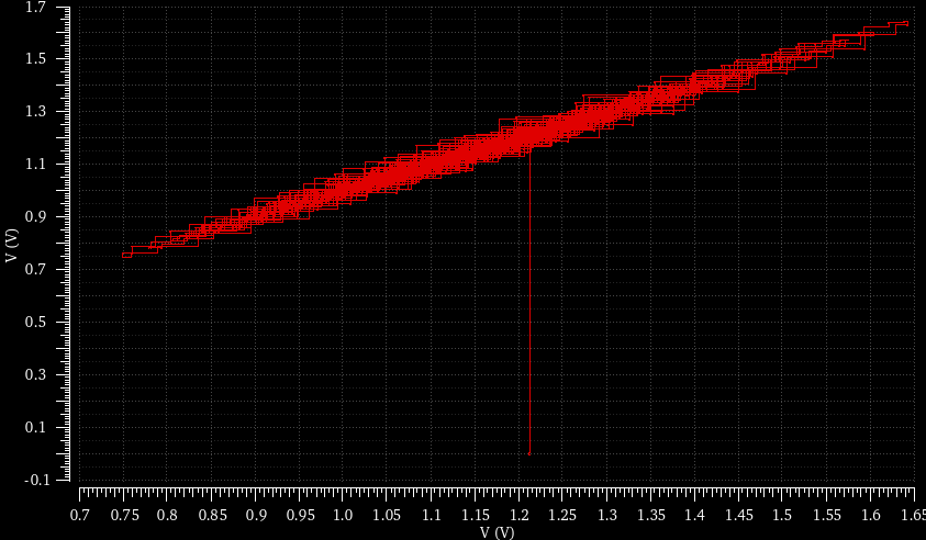
 Final Output/Sampled Input YvsY Curve:
Technical Stack
- Concepts: CMOS, Folded Cascode OTA, Single-Slope ADC, Channel Length Modulation, Transient Analysis.
- Tools: Cadence.